
Offsetting chip variability with Deep Data analytics
As semiconductor processes continue to shrink it’s becoming increasingly challenging to manage the parameters of individual devices not only across the diameter of the wafer, but also across the length of a single chip, especially for a complex chip with a large area. Today’s standard approach to this problem is to assume the worst case and to create a sub-optimal design that accommodates the worst-possible scenario. This no longer needs to be the case.
What does On-Chip Variation (OCV) mean?
Chips are like snowflakes. It would be normal to expect every transistor that is designed the same to behave the same, on a given chip or even wafer. After all, they are all processed in the same manner at the same time, so why should their characteristics differ? But in fact, there are many reasons for these seemingly-identical transistors to differ, and just like snowflakes: although they may look the same at first, close inspection shows that no two are alike. This phenomenon is called on-chip variation (OCV) and it’s caused by several factors.
Process Variation
In an ideal world all semiconductor processes would produce uniform results across the entire wafer. This includes not only the process geometries, which must be patterned to increasingly tight tolerances as processes shrink, but also doping concentrations and film thickness, along with other processes. Imagine the difficulty of assuring a 2nm film thickness ±4% across a 300mm diameter wafer!
Semiconductor tool maker Lam Research illustrated an example of how one process can vary across a wafer with the visual shown below[1]
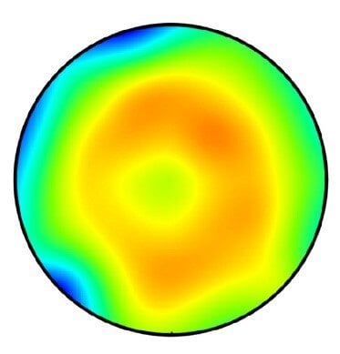
The color gradients illustrate the variation of one of hundreds of processes across the wafer, largely because of differences in the tool’s performance from the edge of the wafer to the center (concentric rings) but also from other factors, which cause the irregular shapes. Lam notes that even the tool’s orientation with respect to the magnetic north can cause irregularities during the plasma etch process.
This image represents a single tool and a single process. A semiconductor wafer is manufactured using over one hundred such processes, so the end result is a wafer with over one hundred such patterns overlaid on top of one another. This means that every transistor across the surface of the wafer has ample reason to perform differently than any of its billions of counterparts.
Although this blog post’s focus is transistors, other circuit elements will also be impacted, including resistors, parasitic capacitance, and even interconnect.
A single chip on this wafer will encompass more than one color in this image, perhaps spanning a green, yellow, and orange zone. A larger chip will have a larger expected variation. This means that transistor performance will vary even across a single chip due to these process variations. Transistors that were designed to be identical might be slower or faster than one another, or leakier or less leaky.
Environmental Variation
Process variation is only one part of the story. In addition to OCV, other aspects affect variability in advanced ICs. A chip by itself is not a uniform operating environment. Different parts of the chip dissipate more power than others, resulting in hot spots within the chip. This is an important consideration during chip design, and layout engineers do their best to even out the heat dissipation across the entire chip. While these engineers do a magnificent job (aided by some amazing CAD tools), a perfect balance can never be reached. The expected operating temperature can be mapped out by the CAD program into a thermal map which uses colors to indicate which portions will run hotter (red) and which will run cooler (blue). An example thermal map, presented by Brown University’s SCALE Laboratory, is in the image below.
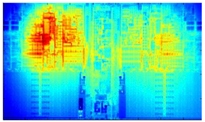
Quite naturally, two identical transistors will operate differently from each other if one is in the red zone while the other is in the blue zone.
These zones are not static – the hot spot will move around depending on the kind of operation that is being performed. Consider a microprocessor chip: If it is performing signal processing, which requires a lot of multiply-adds, then the floating point unit (FPU) of the chip will be doing a lot of computation and consuming a lot of power, so the hot spot will be near the FPU. At some other time the processor might stop doing signal processing and start sorting data. During a sort, the processor does little more than move data into the chip, occasionally check its value, then move it off to a different address in external memory. The hot spot will shift away from the FPU and towards the interface portion of the chip where data is brought in and sent out.
As the hot spot migrates around on the chip our two transistors will see shifting operating environments: First transistor A is cold while Transistor B is hot, then Transistor B will become cold while Transistor A gets hot. Without any way of monitoring these conditions or of understanding how sensitive each transistor is to temperature variations, a chip must be designed to accommodate the absolute worst case: The designer must assume that transistors’ performance varies across the gamut of performance while being subjected to a very broad range of unknown temperatures. This was the industry’s best-known practice before proteanTecs introduced a means of monitoring chip performance deep within each chip.
Measuring these Differences
If a designer can gain some insight about a specific zone’s performance within an individual chip, the design can be made to accommodate the differences and provide the best performance, rather than being designed for the absolute worst case.
This is where Deep Data chip telemetry comes in. proteanTecs monitors chip health and performance using tiny measurement circuits called “Agents” that are embedded in the chip near to the circuits they are monitoring. These Agents are small enough that they can be broadly distributed across the entire chip near strategic locations, without increasing the chip’s size and cost. They then report measurements back to the proteanTecs analytics platform where machine learning algorithms provide thorough assessment, which can be used to adjust the performance of that portion of the chip. This allows manufacturers more visibility into the chip’s operation, and with that comes more control over the chip’s performance.
For example, in a chip with multiple cores, one core can be allowed to run faster while another will be throttled back based on this newfound visibility. This means that the entire chip need not constantly be guard-banded for the absolute worst case scenario as would normally be done using today’s best-known methods, and significantly greater performance can be attained at no additional cost or power consumption.
This approach provides some important advantages:
- Because the Agents are widespread within the chip they can capture data about the entire chip as well as for multiple blocks within the chip. The chip’s manufacturer then gains visibility into the actual variation in multiple strategic locations, during both production and in-field operation.
- The Agents measure data in several dimensions. They are designed to measure phenomena (e.g. leakage) that aren’t captured by today’s best-known methods, most of which focus on delay alone.
- proteanTecs provides insight as to how the OCV and other variability sources impact performance across the chip. Does the variation stem from process? Thermal gradients? Something else? How does it impact different aspects of the chip’s performance?
From Measurement to Insights
The below screen, taken from proteanTecs advanced analytics platform, represents the entire wafer, broken into individual chips. Each chip is covered by a high-coverage and wide-ranging spread of Agents. The colors reveal how an Agent’s measurement compares against the average of all the relevant Agents in the same chip, and is presented on a wafer map.
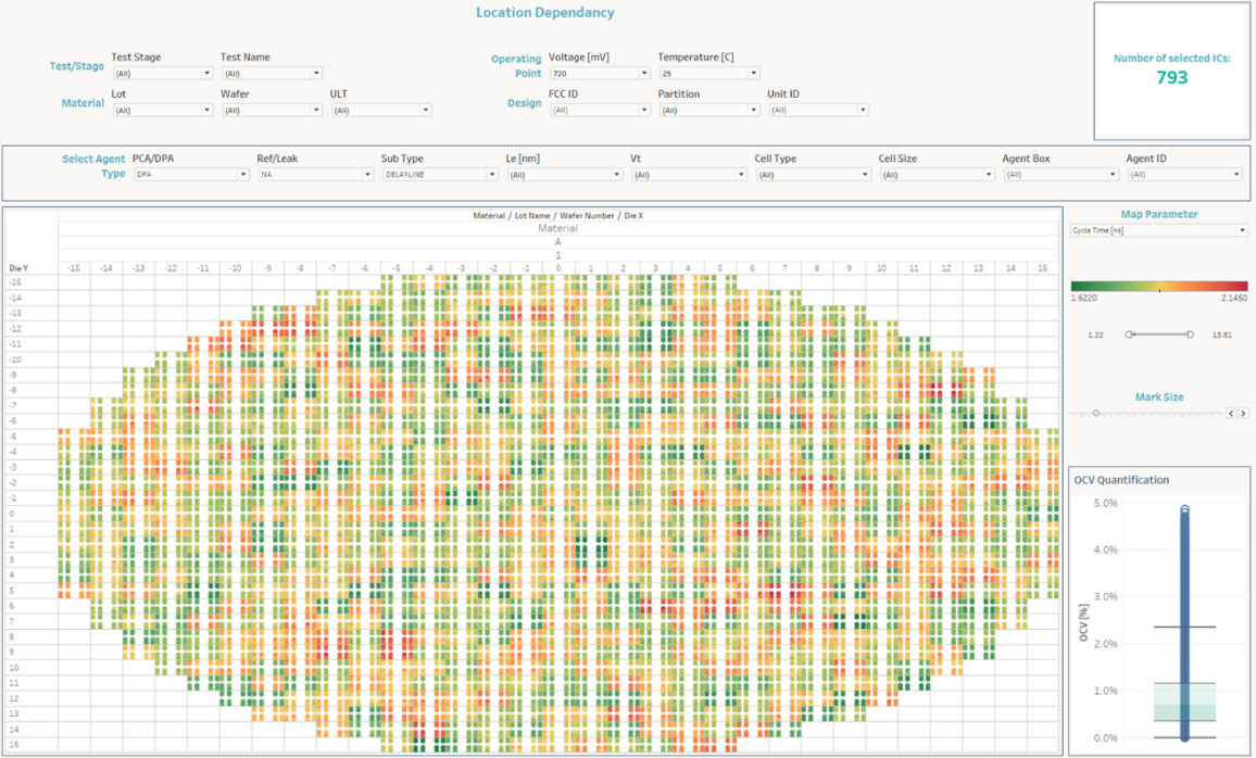
Users can select which Agent or parameter to view in the analytics platform, for a comprehensive and holistic approach.
Below is a detailed parametric view of a single chip, with a wide spread of dots representing embedded Agents. The red dots represent Agents whose values for the selected parameter are significantly below the average, and green dots represent those whose values are significantly above average. The average dots are orange, with other shades representing values between these levels.
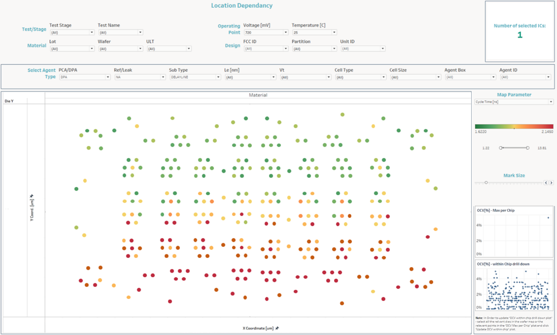
Deep Data chip telemetry provides visibility into operating parameters that cannot otherwise be tested. These are all compared against the same parameter across both the chip and the wafer, to provide valuable insight about how this one chip can be expected to perform in comparison to its peers. Now it’s up to chip manufacturers to find ways to compensate for variations to improve chip performance and reliability.
Who Benefits from This and How?
This kind of information is invaluable to the engineers who are characterizing a new chip design during the new product introduction phase. This team gets a very clear understanding of the chip variability which helps them understand the chip operation. They can then feed this information back to the process engineers, if the problem stems from process parameters, or to the chip’s design team if a design adjustment is warranted. This will help the entire company to improve yields and achieve more uniform behavior across the chip. This high level of measurement resolution creates collaboration across the teams, since they are working to solve understood issues, rather than guessing at the cause of their problems.
Continuous visibility of variation also helps engineers to determine whether a specific chip is likely to suffer a field failure, and whether certain circuits are more likely than others to be the cause of that failure. This allows qualification engineers to learn if a part of the chip should be redesigned. Deep Data helps to identify potential problem areas to make smarter decisions which will reduce or eliminate field failures.
After the device enters production, the system-level or application-level designers can use the same approach to make better decisions about how to use the chip. They can now deeply understand how strong a chip variation really is and how it impacts the chip’s performance in the actual application.
Conclusion
Advanced processes can result in significant chip variation that is not sufficiently measured by today’s standard techniques. Advanced chips that embed high-coverage Deep Data telemetry can be made to reveal a high-resolution look at their internal performance and how it is impacted by this variation. Armed with this data, chip designers can improve their designs to compensate, process engineers can improve their process to reduce OCV, and application engineers and system designers can tune the system not only to improve performance, but also to gain visibility into potential failures before they happen.
[1] Evolution of across-wafer uniformity control in plasma etch,Semiconductor Digest, August 2016
https://sst.semiconductor-digest.com/2016/08/evolution-of-across-wafer-uniformity-control-in-plasma-etch/#


